Customer Service
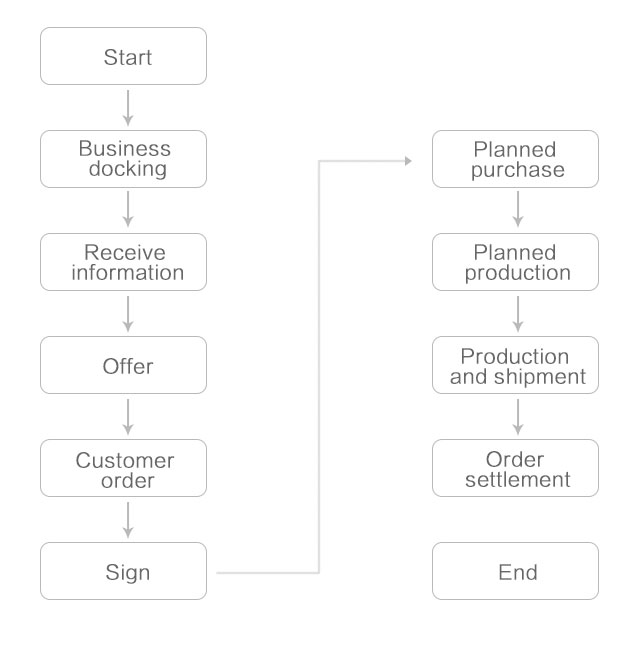
Service Flow

Common Problem
1.What information do PCBA processing need to provide?
Electronic version controlled BOM files, PCB files, GERBER files, PDF location map, special welding requirements, etc.
2.PCBA routine processing flow?
Printing - patch - reflow -AOI inspection -QC sampling - plug-in - wave soldering - repair welding - Cleaning - general inspection -ICT-FCT-OQC- packaging
3.What are the requirements for the PCB production routine?
1. the process edge 5mm (especially the PCB plate edge has device plate, special shape plate) and the process edge needs to increase in the long side of the 2. diameter 1-1.5mm MARK point, to ensure the accuracy of the mounting; 3. if the tailor board, it is necessary to pay attention to the splicing way, such as too much splicing board or V cutting too deep, easy to cause PCB plate change shape.
4.What do you want to do?
1.PCB board components number 2.PCB board size less than 50mm must do the puzzle. 3. before making a plate, we should contact our technology and communicate with each other.
5.How to control the quality of welding?
According to the industry IPC-610A-F standard and customer special requirements, strict control and control from human, machine, material, law and ring are carried out. The specific welding quality control and control should be defined according to different PCB boards.
6. In which case is the design of PCB board unreasonable, which leads to poor welding?
There can be no holes on the 1.PCB welding plate. As the tin inflows into the hole, the size of the weld plate of the solder less tin 2. patch is not consistent with the BOM requirements. The size of the large weld plate is small and the size of the small welding disk is large; the diameter of the 3. plug-in plug is small or large or the distance between the two holes is not matched with the material. 4.PCB board components layout, chip and other large devices, plug-in materials should be placed as much as possible TOP surface, BOT as far as possible design resistance capacitance parts.
7.What are the requirements for processing materials for incoming materials?
1. the material is complete, the 2. incoming packaging is clearly described, and there are no deformation, oxidation, overdue and wrong material. 3. as far as possible for vacuum packing
8.In what case is it recommended to increase the soldering of wave peak control tools?
1. double sided patch board, and product plug-in materials are more. 2. has begun to mass production.
9.How long is the delivery date under normal conditions?
After the material is complete, under normal circumstances, according to the production plan, in about 1-2 weeks.
-

- Building 15, No. 3255 Shengang Road, Songjiang District, Shanghai
-

- 021-24208323
-

- info@www.lfocv.cn

-

- Building 15, No. 3255 Shengang Road, Songjiang District, Shanghai
-

- 021-24208323
-

- info@www.lfocv.cn
- Powered by BEIYU
Follow us
